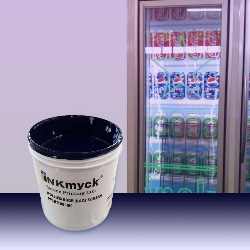
Can Low-Temperature Conductive Ink for Glass Unlock New Smart Device Applications
2025-12-03
The relentless drive for sleeker, smarter, and more integrated devices is pushing design boundaries. A key frontier is the seamless fusion of functionality into glass surfaces. This is where advanced materials like Low-Temperature Glass Ink become pivotal. Inkmyck is at the forefront of this innovation, developing precision-engineered conductive inks that transform ordinary glass into interactive, intelligent components. Unlike traditional high-temperature processes, our technology enables the integration of delicate circuits and sensors onto glass without compromising its structural integrity or optical clarity, directly empowering the next wave of smart device applications.
Engineered for Performance: The Inkmyck Advantage
Our Inkmyck conductive Low-Temperature Glass Ink is not a generic solution; it is a system engineered for high performance in demanding applications. Below are the core parameters that define its capabilities.
Key Product Parameters:
-
Curing Temperature: Cures effectively at temperatures below 150°C, compatible with thermally sensitive substrates.
-
Volume Resistivity: Achieves excellent conductivity as low as 15 mΩ/sq/mil, ensuring efficient signal transmission.
-
Adhesion Strength: Demonstrates superior adhesion to various glass types (>5B as per ASTM D3359).
-
Flexibility: Maintains circuit integrity after repeated bending, crucial for flexible or curved glass designs.
-
Printing Compatibility: Formulated for high-resolution deposition via screen printing, inkjet, and aerosol jet processes.
For a quick technical overview, refer to the table below:
| Feature | Specification | Benefit for Smart Devices |
|---|---|---|
| Curing Profile | < 150°C in 15-30 min | Enables use on tempered, coated, or laminated glass. |
| Conductivity | 15 - 25 mΩ/sq/mil | Ideal for touch sensors, fine-pitch antennas, and heaters. |
| Line Resolution | Up to 50 μm | Allows for miniaturized, invisible circuit integration. |
| Substrate Bonding | Excellent on glass, sapphire | Creates durable interfaces for wearables and automotive displays. |
Low-Temperature Glass Ink FAQ
What are the main advantages of low-temperature curing for conductive ink on glass?
The primary advantages are material compatibility and energy efficiency. Curing below 150°C prevents damage to pre-treated, laminated, or chemically strengthened glass. It also allows for the use of flexible and cost-effective substrate materials, reduces thermal stress, and significantly lowers manufacturing energy costs.
Can Inkmyck's ink be used for transparent antenna applications?
Absolutely. Inkmyck's formulation can be tuned for both opaque and high-transparency conductive patterns. When printed in fine mesh designs, it is excellent for creating transparent 5G antennas, NFC, or RFID circuits on glass windows or displays, maintaining signal performance without obstructing the view.
How does this ink technology enable new smart device designs?
It unlocks the potential for "glass-as-a-device." Designers can now integrate touch controls, environmental sensors, or anti-fog heating elements directly into curved automotive glass, smart appliance surfaces, or wearable device lenses. This facilitates truly seamless, durable, and aesthetically clean human-machine interfaces.
Unlock Your Design Potential
The integration of intelligent functions directly into glass is no longer a futuristic concept. With Inkmyck's high-performance Low-Temperature Conductive Ink for Glass, your path to innovative, integrated, and revolutionary smart devices is clear. Our technical team is ready to support your specific application challenges and help you bring your most ambitious concepts to life.
Contact us today to request a sample data sheet or to discuss a custom formulation for your next-generation smart device project.